Creation of Materials by Super Thermal Field:
Neo-3D printing by Manipulating Atomic Arrangement
through Giant Potential Gradient
We are pleased to announce that the 1st international conference on Creation of Materials by Superthermal Field 2023 (CMSTF2023) will be held at “Yuichi Yamamura Memorial Hall” of Life Science Center in Senri-Chuo, Osaka, Japan from November 15 to 17, 2023.
-
The 16th World Congress on Computational Mechanics (WCCM 2024) is set to be held in Vancouver, Canada, from July 21-26, 2024. Prof. Koizumi will organize a symposium titled “Modeling and Simulation for Additive Manufacturing” alongside Professor Albert To from the University of Pittsburgh. The deadline for submitting abstracts for this symposium is fast approaching on January 15, 2024. Your enthusiastic participation and invitation to others interested are greatly appreciated.
-
The international conference Creation of Materials by Super-Thermal Field (CMSTF 2023) was held.
-
CMSTF2023(2023.11.15~17),Registration for the conference tour has started.
-
CMSTF2023(2023.11.15~17),The conference tour will include a visit to Osaka Castle and a ride on the Aqua Liner (Water Bus) that goes around the castle and the center of Osaka city.
-
The abstract submission of the 1st international conference on Creation of Materials by Superthermal Field 2023 (CMSTF2023) is open.
-
The 16th World Congress on Computational Mechanics (WCCM 2024) is set to be held in Vancouver, Canada, from July 21-26, 2024. Prof. Koizumi will organize a symposium titled “Modeling and Simulation for Additive Manufacturing” alongside Professor Albert To from the University of Pittsburgh. The deadline for submitting abstracts for this symposium is fast approaching on January 15, 2024. Your enthusiastic participation and invitation to others interested are greatly appreciated.
-
The international conference Creation of Materials by Super-Thermal Field (CMSTF 2023) was held.
-
The abstract submission of the 1st international conference on Creation of Materials by Superthermal Field 2023 (CMSTF2023) is open.
-
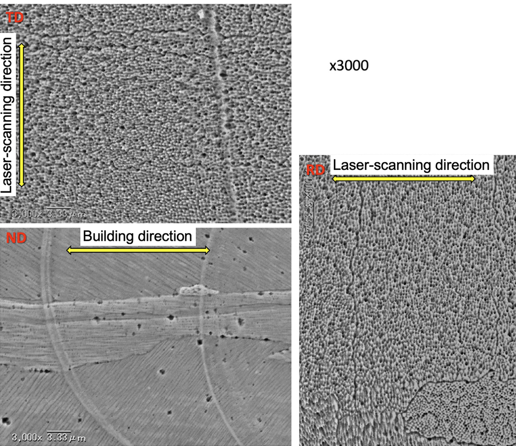
The research results of the A01a group were published in the morning edition of the Nikkan Kogyo Shimbun, “3D modeling clarification of miniaturization: applications for automobiles and aerospace.”
-
The international conference Creation of Materials by Super-Thermal Field (CMSTF 2023) was held.
-
CMSTF2023(2023.11.15~17),Registration for the conference tour has started.
-
CMSTF2023(2023.11.15~17),The conference tour will include a visit to Osaka Castle and a ride on the Aqua Liner (Water Bus) that goes around the castle and the center of Osaka city.
-
The abstract submission of the 1st international conference on Creation of Materials by Superthermal Field 2023 (CMSTF2023) is open.
-
Transformative Areas Super-Temperature Field 3DP Open Symposium will be held on October 26th (Wednesday) (Deadline: October 19th)
Message
Creation of Materials by Super Thermal Field:
Neo-3D printing by Manipulating Atomic Arrangement
through Giant Potential Gradient

Outline of Research
This research area aims to elucidate the mechanism of unique crystal growth that occurs in STF, which is generated by extremely local heating by electron beams or lasers in metal 3DP.
The research includes advanced experimental in-situ observations and analyses such as high-speed optical temperature-field analysis, synchrotron X-ray transmission imaging, high voltage electron microscopy, and associating numerical simulations consistent with those experiments. The numerical simulations include computational thermal fluid dynamics, phase-field methods, and molecular dynamics. Moreover, artificial intelligence is utilized to analyze the correlation of the process-structure-property relationship.
These researches will establish the science for creating new materials by STF, which will contribute to the creation of new materials via the development of new technology such as 3DP of single crystals, and thus, contribute greatly to materials science.
Planned Research
-
Research Group A01-a
Digital Twin Science for the creation of materials Integration of Process Monitoring and Simulation
開く -
Research Group A01-a investigates the melting and solidification behavior in STF in the 3DP process by digital twin science analysis: a combination of in-process monitoring, microstructure observations, computational thermal-fluid dynamics simulations, and phase-field (PF) simulations. Specifically, phenomena unique to STF such as crystal growth under temperature gradients of 10 million K/m and Marangoni convection caused by temperature gradients at liquid phase surfaces are analyzed. This research enables us to predict the optimization of the 3DP process and systematize new scientific knowledge, which will serve as a basis for understanding the behavior of materials in STF.
PI 
Yuichiro KOIZUMI Professor,
Division of Materials & Manufacturing Science,
Graduate School of Engineering,
Osaka UniversityCo-Investigator 
Masayuki OKUGAWA Assistant professor,
Division of Materials & Manufacturing Science,
Graduate School of Engineering,
Osaka UniversityCollaborator 
Yasushi SHIBUTA Professor,
Department of Materials Engineering,
School of Engineering, The University of TokyoCollaborator 
Munekazu OHONO Professor,
Faculty of Engineering,
Division of Materials Science and Engineering,
Hokkaido UniversityCollaborator 
Shuhei ICHIKAWA Assistant Professor,
Division of Electrical,
Electronic and Infocommunications Engineering,
Graduate School of Engineering,
Osaka UniversityCollaborator 
Shuhei HATANAKA Technical Staff,
Research Center for Ultra-High Voltage Electron Microscopy,
Osaka UniversityCollaborator 
Yuheng LIU Specially Appointed Assistant Professor,
Graduate School of Engineering Division of
Materials and Manufacturing Science,
Osaka University-
In-process monitoring using a high-speed camera
Emitting light from melting and solidifying materials by a laser or electron beam scanning at a high speed of over 1 m/s is captured by a high-speed camera with a temporal resolution of less than 1/100,000 of a second. Obtained images are analyzed to measure the temporal variation of the surface temperature distribution to understand the relationship between the interaction of various beams with materials and the generation of STF, and to improve the agreement between computer simulations and experiments.

High-Speed Camera Images of Metal Melted by Laser Scanning

Surface Temperature Distribution Image obtained by Two-Color Method of High-Speed Camera Imag
-
Crystal Growth Simulation by Phase-Field Method
Crystal growth simulations in STF using the phase-field method are performed. The simulations use parameter determination by data assimilation in collaboration with Research Group A01-b, which is in charge of materials informatics in this Transformative Research Areas (A). We simulate directional solidification in STF by focusing on the solute distribution changes associated with solid-liquid interface velocity and optimize solidification conditions for single crystal growth, including epitaxial growth with absolute stability. The conditions used for Research Group A03’s building experiments.
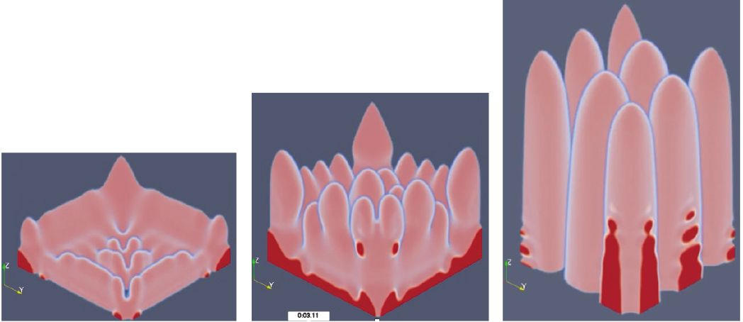
Crystal Growth Simulation by Phase-Field Method
-
Computational Thermal Fluid Dynamics (CtFD) Melting and Solidification Simulation
CtFD simulation combined with in-process monitoring (Digital-twin analysis) is used to obtain the temperature gradient (G), solidification velocity (R), flow velocity (U), and the direction of solid-liquid interface migration (Φ), which are difficult to obtain experimentally, to identify the effect of STF on nano and microstructure formations that determine the properties of materials.
CtFD Simulation of Melting and Solidification from Laser Beam Scanning
-
Molecular Dynamics Simulation of Solid-Liquid Interface
Research Group A01-a performs molecular dynamics simulations of solid-liquid interface migration to determine the interfacial mobility for phase-field crystal growth simulations in collaboration with Research Group A01-b. Solute distributions in STF, which are significantly different from conventional solidification processes, are analyzed to evaluate changes in solute partition coefficients as the solidification rate increases.
Molecular Dynamics Simulation of Solid-Liquid Interfaces
-
-
Research Group A01-b
Materials Informatics in STF Discovering Laws and Optimization Predictions from Big Data
開く -
To bridge experimental and simulation research using materials informatics, Research Group A01-b undertook the following missions: Forward and inverse analysis: This enables the derivation of microstructures that exhibit the desired properties and the process conditions that create those structures, and it clarifies the physics behind these laws.
Data assimilation: These are methods, including the adjoint method, used to efficiently determine physical property parameters, such as mobility and interfacial engineering parameters, that are required for (CtFD) and phase-field simulations.
3D observations: These are quantitative evaluations of structural features based on 3D observation results.PI 
Yoshitaka ADACHI Professor,
Department of Materials Design Innovation Engineering,
Graduate School of Engineering,
Nagoya UniversityCo-Investigator 
Akiori YAMANAKA Professor,
Division of Advanced Mechanical Systems Engineering,
Institute of Engineering,
Tokyo University of Agriculture and TechnologyCollaborator 
Nobuo NAKADA Professor,
School of Materials and Chemical Technology,
Tokyo Institute of TechnologyCollaborator 
Asuka SUZUKI Assistant professor,
Materials Process Engineering,
Graduate School of Engineering,
Nagoya UniversityCollaborator 
Fei SUN Specially Appointed Associate Professor,
Department of Materials Design Innovation Engineering,
Graduate School of Engineering,
Nagoya University-
Research Objectives of Research Group A01-b
Materials informatics are used to bridge experimental and simulation studies. Specifically, in collaboration with Research Groups A01-a, A02, and A03, Research Group A01-b work on the automatic collection and interpolating of necessary data, thorough quantitative structure analysis, forward and inverse analysis of process optimization to obtain desired structures, and data assimilation to improve the accuracy of simulations.
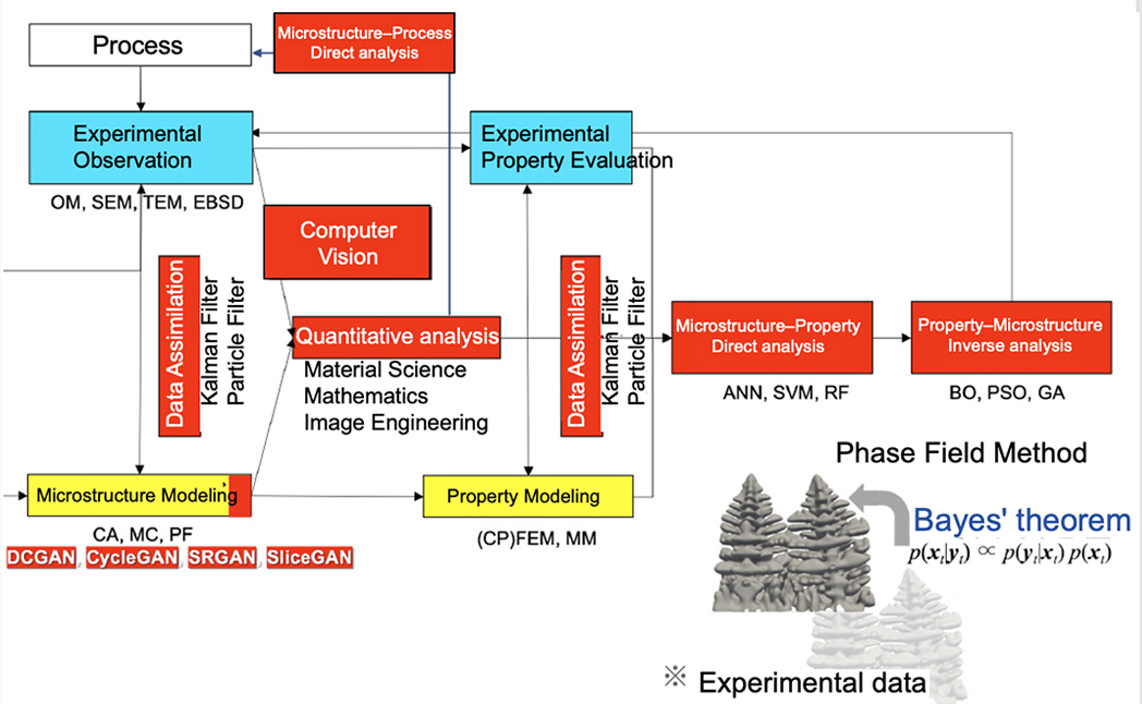
Overall View of Materials Informatics (MI)
(Blue: Experimental; Yellow: Simulations; Red: Data Science)
*Data assimilation linked advanced in-situ observations and phase-field simulations -
Ongoing Research Projects
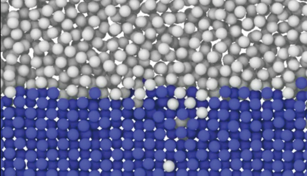
- Ultrafast 3D Structure Image Techniques Using State-of-the-Art Adversarial Generative Networks
- Development of Cube Polisher
- High-Resolution 3D Image Acquisition by Serial Sectioning/EBSD
- Analysis of Phase Equilibrium Behavior by State Diagram Calculation
- Data Assimilation
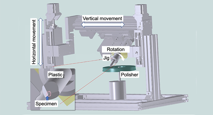
Cube Polisher Design Diagram
Results of Three-Sided Observations
-
-
Research Group A02-a
Microdynamics of Crystal Growth in STF In-Situ Observation by Time-Resolve X-Ray Imaging
開く -
Research Group A02-a observe in-situ extremely rapid local melting and crystallization during in metal 3DP processing by using synchrotron radiation X-ray imaging with micro-ordered time and spatial resolution. This research group obtain quantitative observation and measurement data on the solidification rate, its change, and the growth direction in the melt pool and liquid phase flow, including Marangoni convection and solute transportation caused by the flow. This research group also clarify the microdynamics of crystal growth in STF including the interaction in the surrounding environment, such as between the existing built structure and the melt pool and between the melt pool and the metal powder. Working with Research Group A01-a, which was in charge of digital twin science and materials informatics, the aim of Research Group A02-a is to reveal the fundamentals of crystal growth in STF.
PI 
Kohei MORISHITA Associate Professor,
Department of Materials,
Kyushu UniversityCollaborator 
Kentaro UESUGI Chief Scientist,
Scattering and Imaging division,
Japan Synchrotron Radiation Research InstituteCollaborator 
Hideyuki YASUDA Kyoto University,
Deprtment of Materical Science and Engineering,
Graduate School of Engineering,
Professor-
Targeted Microdynamics and Scale in Crystal Growth in STF
Rapid melting by laser irradiation and subsequent crystal growth are greatly affected by non-equilibrium and non-static phenomena, such as melting behavior on the already built layers, Heat-flow, interactions with surrounding powder, and shape changes of the melt pool. This Research Group clarify the microdynamics at the melt pool scale in STF including the interaction with the surrounding environment.
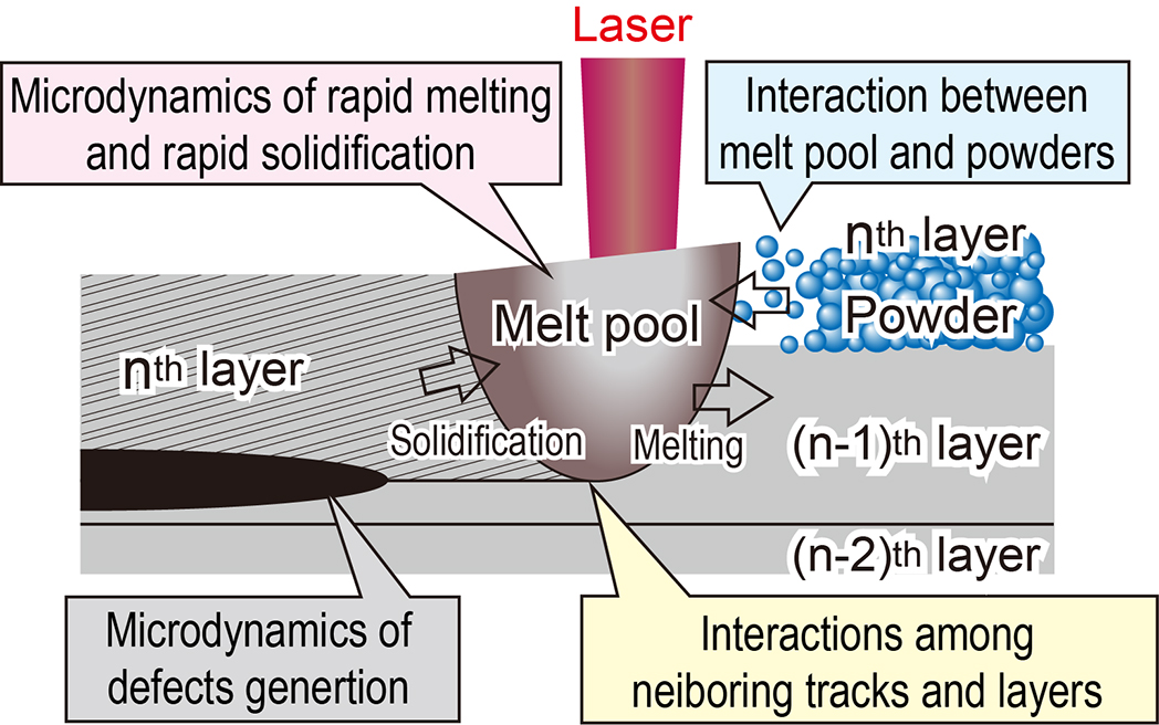
Microdynamics Occurring at Melt pool Scale
-
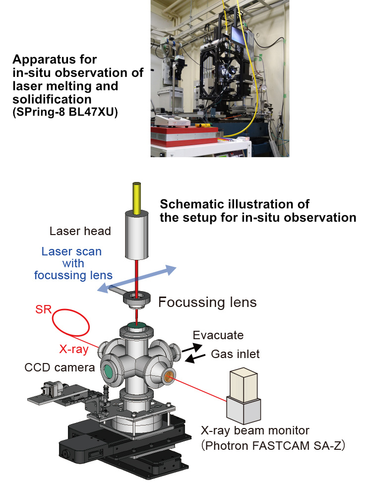
In-Situ Observation of Rapid Melting and Rapid Solidification Behavior Using Synchrotron Radiation X-Ray Imaging
Using the large-scale synchrotron radiation facility, SPring-8, X-rays with a wavelength to obtain appropriate absorption for alloys are transmitted to a sample undergoing rapid melting and solidification. By capturing the density differences between the liquid and solid phases, the solid-liquid fraction, and the absorption contrast, depending on the solute distribution, in-situ observations, with a temporal resolution of 50 µs and a spatial resolution of 1 µm to sub-µm, are performed.
-
Rapid Melting and Rapid Solidification Behavior by Laser Irradiation
The research found the completely melting area, solid-liquid coexistence area, and solidified area following the laser scanning. The figure shows a slow scanning speed of 5 mm/s. In the near future, this Research Group will observe the phenomena at scanning speeds in units of meters per second using a galvanometer scanner. It will also clarify the relationship between the melt pool shape and the solidification microstructure by spot laser irradiation for milliseconds to sub-milliseconds.
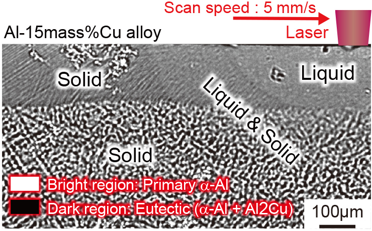
In-Situ Image of Al-15mass%Cu Alloy
The light region shows the original primary α-phase, and the dark region shows the eutectic. -
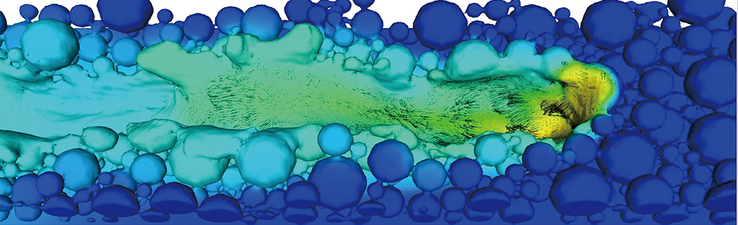
Liquid Flow Induced by STF
STF generates Marangoni convection by creating large surface tension gradients. The figure shows convection observed from the movement of a gas-bubble captured inside a melt pool of copper powder. The research will empirically clarify how unsteady liquid flow correlates with the formation process of a melt pool and its shape and solidification, including the effects on heat, mass transport, and fusion.
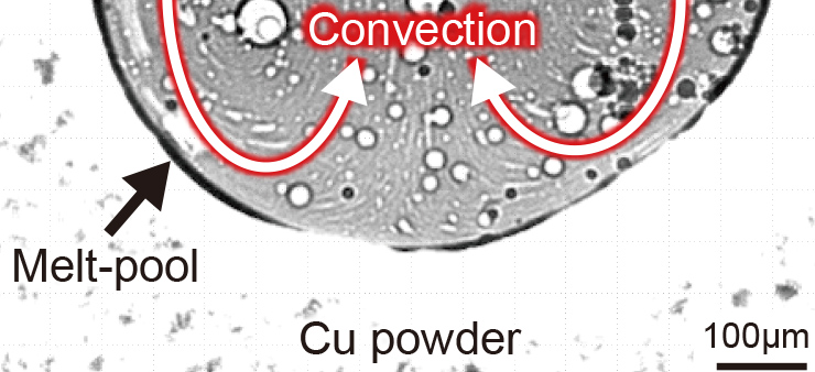
Convection in Melt pool Formed by Laser Irradiation on Cu Powder
-
-
Research Group A02-b
Lattice Defects Analysis in STF Advanced Analytical Materials Science
開く -
There are unsolved questions about crystal growth in 3DP, such as the huge temperature gradients that never occur in conventional melting and solidification processes. Therefore, Research Group A02-b focuses on a combined and unified analysis of the morphology, strain, and vacancy (lattice defects analysis in STF) using advanced analytical methods (high-voltage electron microscopy, neutron diffraction, and positron annihilation). The aim is to clarify the 3D microstructure and composition, the stress and strain fields, and the lattice defects of alloys formed by the powder bed fusion (PBF) method and then establish a material microstructure science that would contribute to the systematization of 3DP.
PI 
Kazuhisa SATO Associate Professor,
Research Center for Ultra-High Voltage Electron Microscopy,
Osaka UniversityCo-Investigator 
Ken CHO Associate Professor,
Division of Materials and Manufacturing Science,
Graduate School of Engineering,
Osaka UniversityCo-Investigator 
Masataka MIZUNO Associate Professor,
Center for Atomic and Molecular Technologies,
Graduate School of Engineering,
Osaka UniversityCollaborator 
Hiroyuki YASUDA Professor,
Division of Materials and Manufacturing Science,
Graduate School of Engineering,
Osaka UniversityCollaborator 
Satoshi ICHIKAWA Specially Appointed Professor,
Research Center for Ultra-High Voltage Electron Microscopy,
Osaka UniversityCollaborator 
Shunya TAKAGI Specially Appointed Researcher,
Research Center for Ultra-High Voltage Electron Microscopy,
Osaka University-
Three-Dimensional Structural Analysis of Microstructures Using High-Voltage Electron Microscopy
This Research Group utilize the latest high-voltage electron microscope and a state-of-the-art electron direct detection CMOS camera to reveal the distribution, shape, and density of micro-precipitates and nanopores in 3DP materials as well as the microstructure and composition of the melt pool periphery. Research Group A02-b will attempt to visualize the microstructure and composition distribution of a thick film sample in 3D reflecting the shape of the melt pool by using high-voltage electron microscopy and the latest analytical techniques.
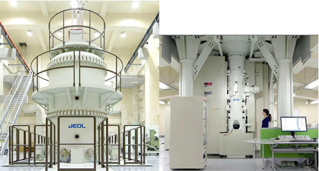
Materials and bio-science high-voltage electron microscope (installed at Osaka University’s Research Center for Ultrahigh Voltage Electron Microscopy in FY2015)
The microscope is equipped with an electron direct detection CMOS camera, STEM, an energy filter, and the world’s first cryostage (currently operating with a conventional pole piece) with a maximum acceleration voltage of 1,250 kV. Sample two-axis tilt, sample heating/cooling, and electric-field-applied observation are available. -
Detection of Lattice Defects by Positron Annihilation Method
Positron lifetime measurements, which can detect lattice defects with high sensitivity, were used to evaluate and analyze lattice defects introduced by STF in 3DP materials. The relationship between the types and concentration of lattice defects, process conditions, the specimen shapes and sizes are studied. Positron lifetime component analysis and first-principles calculations are also used for the detailed analysis and stability evaluation of lattice defects.
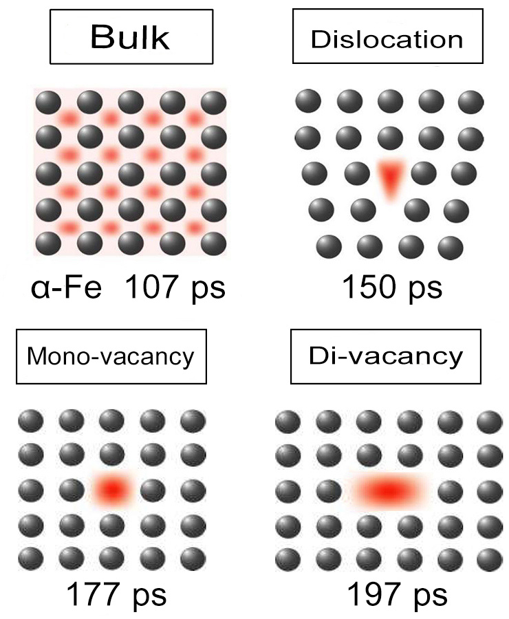
Distribution of Positron Density and Positron Lifetime Values in Pure Iron Because the positron lifetime is inversely proportional to the electron density at the annihilation site, and varies with the annihilation site, the type of lattice defect can be identified. Quantitative evaluations of vacancy concentration are also possible through positron lifetime component analysis.
-
Quantitative Analysis of Stress and Strain Fields by Neutron Diffraction
Neutron diffraction is used to quantitatively analyze the stress and strain fields inside 3DP materials fabricated at various conditions to reveal their macroscopic three-dimensional distributions. Furthermore, the effects of the solidification conditions, temperature distribution, etc. on forming stress and strain fields are elucidated by combining micro-scale electron backscatter diffraction analyses.
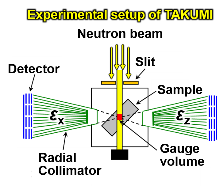
Schematic drawing of theBL19 TAKUMI Engineering Materials Diffractometer at the Japan Proton Accelerator Research Complex (J-PARC), Japan Atomic Energy Agency (JAEA). Pulsed neutron beam is injected into the sample, and neutron diffraction pattern is measured by a pair of detectors facing each other. Diffraction profiles in two directions can be obtained simultaneously. Therefore, two strain components can be analyzed simultaneously.
-
-
Research Group A03-a
Science for Super-Titanium Creation in STF New Microstructure Design of Heat-Resistant Titanium Alloys with Property Improvements using STF
開く -
Research Group A03-a focuses the single crystallization and grain refinement of titanium alloys that are used for jet engine materials under STF to improve the properties of the materials. The aim is to clarify the crystal growth and phase transformation behavior of titanium alloys by 3D additive manufacturing to control their structures and improve their properties. In particular, this Research Group creates structures that take advantage of microstructural refinements in STF generated during laser and electron beam melting and reveals the melt and solidification process to improve mechanical properties.
PI 
Yoshiaki TODA Principal Researcher,
Research Center for Structural Materials,
High Temperature Materials Design Group,
National Institute for Materials ScienceCo-Investigator 
Takayoshi NAKANO Professor,
Division of Materials & Manufacturing Science,
Graduate School of Engineering,
Osaka UniversityCo-Investigator 
Yoko MITARAI Professor,
Department of Advanced Materials Science,
Graduate School of Frontier Sciences,
The University of TokyoCo-Investigator 
Tetsuya MATSUNAGA Associate Professor,
Institute of Space and Astronautical Science,
Japan Aerospace Exploration AgencyCollaborator 
Ryosuke OZASA Assistant professor,
Division of Materials & Manufacturing Science,
Graduate School of Engineering,
Osaka University-
Microstructure and High-Temperature Properties of Heat-Resistant Titanium Alloys by Conventional Processes
Titanium has about half the density of nickel and iron and has a specific strength superior to nickel-based alloys at temperatures below 600°C. Using the advantage, heat-resistant titanium alloys are used in some jet engine components. But it is necessary to make high-temperature property improvements to expand the application temperature range of titanium alloys for energy efficiencies. The microstructural morphology of β-phase (body-centered cubic structures) and α-phase (hexagonal close-packed structures) must be controlled to improve high-temperature properties. The conventional post-forging heat treatment process form an equiaxed α-phase microstructure or a layered α/β microstructure. The former is effective in improving fatigue properties and the latter in improving creep properties. However, it is difficult to improve both properties. Although the conventional process creates bimodal structure, i.e., a mixture of the equiaxed α phase and the layered α/β phases, showing the good balance of these properties, improvements in microstructure control and the high-temperature properties have reached their limits by conventional processes.
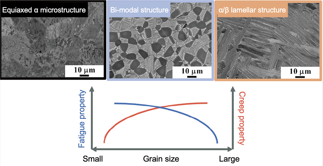
Relationship between Microstructures and Fatigue/Creep Properties of Heat-Resistant Titanium Alloys Obtained by Conventional Forging Processes
-
Additive Manufacturing in STF
This study applies STF with steep temperature gradient and fast cooling rate to retaining a β-phase solid solution after the cooling process dropped to room temperature and to controlling a crystal orientation of the material. The phenomena will lead to a single-crystal β titanium alloy which has never been achieved before.
This could enable to generate a lamellar microstructure in which an α phase is precipitated from the β phase with a single orientation, creating new titanium materials that would exhibit excellent high-temperature strength for jet engine rotors. It reveals importance of STF to create new super titanium alloys with single-crystal matrix or microstructures which cannot be formed by the conventional processes.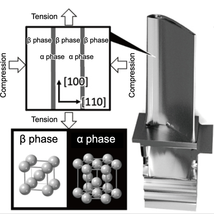
Image of Super Titanium Created using STF
The lamellar microstructure, which is created when the α-phase is precipitated from the single β-phase in one orientation, improves the high-temperature strength in the centrifugal direction of a rotating body. -
Computational Search for Conditions of Optimal Precipitation Morphology
This Research Group searches alloy compositions and heat treatment conditions to obtain an optimal precipitation morphology of the α-phase that would improve the properties of the material. A simple model describing precipitation phenomena and energy computation are used to predict the precipitation and growth process of the α-phase precipitated from the single β-phase obtained in a STF. This Research Group expects that recent computational search technique becomes a powerful tool to reveal the optimal precipitation morphology in various alloy compositions and heat treatment conditions.
Example of Energy Computation Predicting α-Phase and Third-Phase Precipitation from the Single β-Phase of a Titanium Alloy
-
-
Research Group A03-b
Science of Biomaterials Creation Utilizing STF Creation of Materials for Manipulating Biological Functions by 3DP STF
開く -
Research Group A03-b conducts scientific research, using STF generated by 3DP, to create highly functional devices from both 'surface' and 'bulk' perspectives, with the specific target of biomaterials for use in bone. Specifically, the atomic arrangement and their orientation are precisely controlled, while morphological and chemical modifications fo0r cellular control are applied to the surface to obtain a biomaterial that can artificially manipulate the bio-functionalities of bones. Furthermore, an index is formulated for evaluating the functionality of biomaterials in vivo.
PI 
Takuya ISHITO Professor,
Aluminium Research Center,
University of ToyamaCo-Investigator 
Masato UEDA Professor,
Materials and BioengineeringDepartment of Chemistry and Materials Engineering,
Faculty of Chemistry,
Kansai UniversityCo-Investigator 
Aira MATSUGAKI Associate Professor,
Division of Materials & Manufacturing Science,
Graduate School of Engineering,
Osaka University-
High Functionalization of Biomaterials Using STF
Research Group A03-b aims to create "STF biomaterials" as one of the outlets for social implementation of "3DP-STF materials" created by utilizing the STF that can only be achieved by 3DP. Specifically, this study targets biomaterials for application in bones. Biomaterials should express their functions in proactive interactions with living tissues. This research aims to introduce a mechanism that enables the action on biological tissues from both “bulk” and “surface” perspectives into metallic biomaterials by utilizing STF. (Fig. 1).
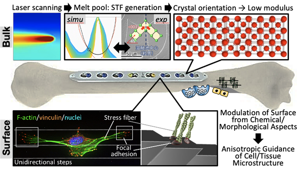
Fig. 1 Conceptual Diagram of the Functionalization of Biomaterials from Bulk and Surface (Interface with the Organism) Perspectives by Controlling STF Unique to 3DP
-
Functionalization from Bulk Perspective Using STF
With the aim of creating an implant device that will suppress bone degradation by stress shielding, this Research Group focuses on the relationship between STF and β-phase instability, and the evolution of crystallographic orientation in STF (Fig. 2) for a β-type titanium alloy. The conditions of STF for a lower Young’s modulus are also explored.
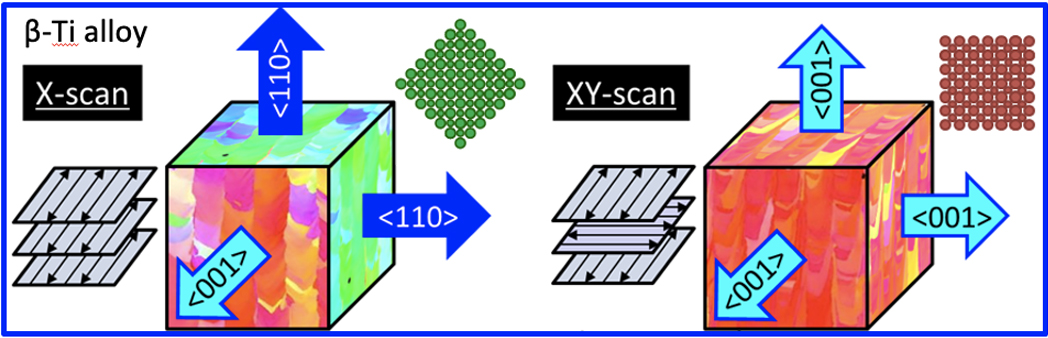
Fig. 2) Crystal Orientation Evolution in STF Depending on Scanning Strategy
The arrow length indicates Young’s modulus depending on the crystallographic orientation. -
Functionalization from Surface Perspective Using STF
The mechanism of bio-functionalization at the surface is combined with that in the bulk. Surface modification is based on both chemical and morphological perspectives. From a chemical point of view, the semiconductor properties of oxides on the STF material surface are utilized (Fig. 3). From a morphological point of view, the spontaneous formation of surface patterning by STF are controlled. This Research Group attempts to control the cell adhesion and the cellular arrangement for normal biological tissue induction by chemical and/or morphological patterning with scales of cell body and cell process using 3DP. The final aim is to fabricate the bulk and surface into a single piece and then evaluate its functionality as a biomaterial through in vitro and in vivo testing. This approach is a novel concept distinct from the conventional 3DP approach to biomaterial development, which is based on controlling complex three-dimensional shapes.
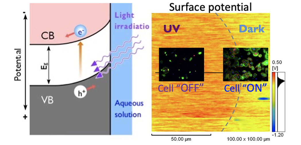
Fig. 3) Control of Surface Potential by UV Irradiation on TiO2.
Cell presence/absence control is expected to be possible with TiO2 patterning.
-
-
Research Group A03-c
Science for Creation of Ceramic Materials by Super Thermal Field A New Horizon for Ceramics Manufacturing Processes by STF
開く -
Research Group A03-c will advance the basic scientific understanding of STF process phenomena aiming at creation of new processes for ceramic manufacturing. By high-intensity laser irradiation, STF is generated inside or on the surface of ceramic objects. In “STF sintering”, densification and crystal growth behaviors in STF are investigated, and in-situ observation of STF sintering is also challenged. In “STF chemical vapor deposition”, mechanisms of enhancement of deposition rates and formation of unique microstructures of ceramic coatings in STF is investigated. In “STF powder spray deposition”, understanding of the joining mechanism of dissimilar materials under STF, and application to practical ceramic coating processes will be progressed.
PI 
Teiichi KIURA Senior Researcher,
Japan Fine Ceramics CenterCo-Investigator 
Takeshi YOSHIKAWA Professor,
Division of Materials & Manufacturing Science,
Graduate School of Engineering,
Osaka UniversityCo-Investigator 
Kentaro SHIODA Leader,
Advanced Functional Surface Group,
Advanced Manufacturing Research Institute,
National Institute of Advanced Industrial Science and Technology (AIST)Co-Investigator 
Akihiko ITO Associate Professor,
Faculty of Environment and Information Sciences Division of Artificial Environment and Information,
Yokohama National University-
Creation of STF Ceramic Sintering Technology Using Lasers
High-intensity laser irradiation generates STF in ceramics green body due to local heat generation near grain boundaries. This STF sintering process causes quite different microstructures from those by conventional sintering process using an electric furnace; extremely rapid crystal growth, strong bonding between grains, and anisotropic shrinkage in the direction of the laser irradiation. Therefore, the aim of this study is to clarify the mechanism of formation of unique microstructures.
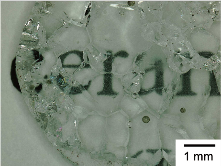
Example of Laser-Sintered Transparent Alumina Body
-
Understanding STF Process Phenomena by Crystal Growth Monitoring
High-speed sintering technology using laser irradiation on alumina fine particle layers is superior in terms of high productivity and is highly compatible with the 3DP process. In addition, the technology is expacted to apply for other materials. However, neither the heating mechanism nor the sintering mechanism under laser irradiation has yet been elucidated. In this study, we will observe the in-situ heating behavior of alumina particle layers coated on sapphire substrates under laser irradiation and the homo-growth rate on sapphire substrate from the particles using a high-temperature microscope to understand the heating behavior and sintering mechanism.
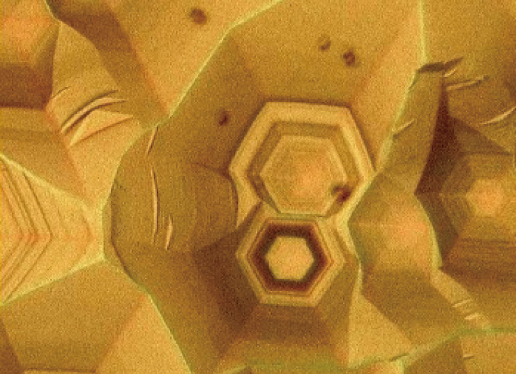
Example of In-Situ Observation of Crystal Dissolution Front
-
Creation of STF-CVD Process Using Lasers
CVD is a coating process of functional and hard materials using a chemical reaction of precursor gas on the surface of the substrate. In STF CVD, laser irradiation can inject energy directly in CVD process, and this is an active chemical reaction field that cannot be reached by the conventional CVD under thermal equilibrium condition. We have found that the self-organization of nanostructures occurs in this process; however, its formation mechanism and microstructural evolution during CVD process remains unclear. This research contributes to the scientific construction of ceramics process science in STF through the in-situ observation of nanostructure formation from the gas phase in STF CVD.
-
Creation of Ceramic Materials in STF by Spraying Fine Particles Under Laser Irradiation
Plasma assistance has proven to be an effective tool for expanding the process window of the fine particle spray deposition of brittle materials, such as ceramics. However, our understanding of the effect of injected energy on the particle bonding and interface creation was insufficient, which has limited the development of new materials. In this study, this Research Group will explore the nature of the interface formation and bonding in the fine particle spray process by utilizing STF created by a laser that has a higher local energy density than plasma. Obtained guidelines for interface control will contribute to create new ceramic coatings as well as new additive manufacturing process of ceramics.
-
Access
| Address |
2-1 Yamadaoka,Suita,Osaka 565-0871,Japan EMAIL: s3dp@mat.eng.o saka-u.ac.jp TEL:06-6879-7477 |
|---|